Affordable solution for nanoscale mapping of electrical measurements, PrimeNano product
sMIM
Scanning Microwave Impedance Microscopy (sMIM)
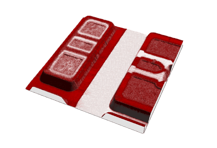
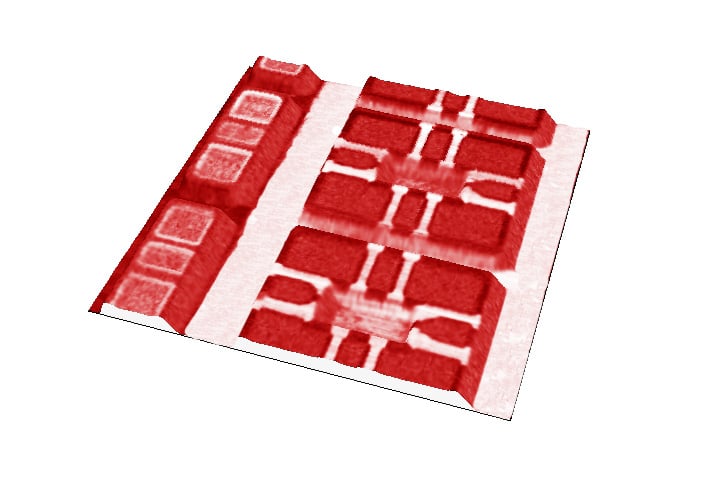
This new AFM mode, developed by PrimeNano, measures the electrical properties of materials at length scales from 10’s of nanometers to microns. sMIM modules produce high quality images of local electrical properties with better than 50 nm resolution.The core of our technical approach is to utilize microwave reflections from a nm scale region of the sample directly under the sMIM probe.
![]() Sensitivity to metals, semiconductors and insulators including dielectrics
Sensitivity to metals, semiconductors and insulators including dielectrics
![]() Direct measure conductivity σ & ε permittivity at the Nano-Scale
Direct measure conductivity σ & ε permittivity at the Nano-Scale
![]() Linear relationship to electrical properties
Linear relationship to electrical properties
![]() Quantitative doping concentration mapping
Quantitative doping concentration mapping
![]() Nano-Scale C-V spectra
Nano-Scale C-V spectra
![]() Sub-surface sensing capability
Sub-surface sensing capability
ScanWave a PrimeNano Inc. product,
More info about PrimeNano & product >>
Applications
![]() Micro-electronics
Micro-electronics
![]() Nano-materials
Nano-materials
![]() Doping profiles
Doping profiles
![]() Biomedical
Biomedical
![]() Green Energy
Green Energy
![]() Photonic materials and devices
Photonic materials and devices
Principle
“Conductivity, Permittivity & N-Doping Concentration.”
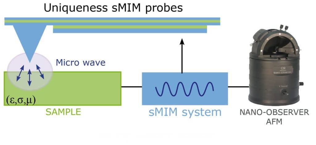
How ScanWave™ Works
- ScanWave™ sends microwaves to the probe tip via a fully shielded path.
- The microwaves create a near-field electromagnetic wave at the the probe tip that interacts with the sample surface and subsurface.
- After the near-field interacts with the sample, a portion of the microwave power is reflected back through the same shielded path to the ScanWave™ electronics for filtering, demodulating, and processing.
- As the probe moves across the sample, the reflected microwaves vary in amplitude and phase due to variations in the local electrical properties under the probe tip.
- The ScanWave™ software calibrates the reflected signal from the probe-sample interface to create a capacitive and a resistive image that are displayed by the AFM simultaneously with the topography image or images.
ScanWave Advantages
“Affordable solution for Nanoscale Mapping of electrical measurements.”
Unprecedented Sensitivity
Industry’s highest sensitivity lets you image the hard stuff. Industry’s lowest noise floor lets you see the small stuff.
Subsurface Imaging
Imaging of buried structures underneath the sample surface is possible thanks to the long range nature of sMIM.
No Conductive Path Needed
No ground or conductive path needed to get your electrical characterization.
Single scan – 6 channels of data
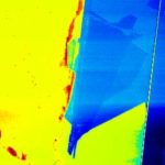
![]() sMIM-C: Capacitance/Permittivity variation
sMIM-C: Capacitance/Permittivity variation
![]() sMIM-R: Resistivity/Conductivity variation
sMIM-R: Resistivity/Conductivity variation
![]() dC/dV Amplitude: Carrier concentration
dC/dV Amplitude: Carrier concentration
![]() dC/dV Phase: Carrier type +/-
dC/dV Phase: Carrier type +/-
![]() dR/dV Amplitude: Carrier concentration
dR/dV Amplitude: Carrier concentration
![]() dR/dV Phase: Carrier type +/-
dR/dV Phase: Carrier type +/-
Minimal Sample Prep Time
Since it is not necessary for the sample to be in a conductive path or under current flow or even for the feature of interest to be exposed, samples can be imaged with minimal prep tim
Contact and Non-Contact Mode Imaging
Electrical measurements can be made in tapping contact imaging modes, even during force distance curves. However you want to scan, ScanWave™ can get the electrical data you need.
Nano Resolution
Transform your AFM into a high resolution, nanoscale local electrical property microscope.
Simultaneously
Be it conductors, semi-conductors, dielectrics, or insulators, ScanWave™ can handle it all. Different materials, even of different classes, can be imaged in the same scan.
Easy to Use Software
Scan management and configuration is a bliss.
sMIM probes
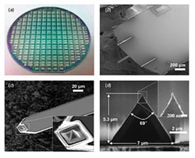
The sMIM probes are batch fabricated MEMS devices (micro electrical mechanical systems) with a shielded front and backside and center transmission line.The probe shielding reduces stray coupling from the environment and the cantilever. The probe radius is nominally 50nm to optimize signal strength and lateral resolution.The probe sample interface use a resistor and capacitor in parallel. This “leaky capacitor” presents an impedance mismatch to the 50 ohm system electronics, creating a reflection.
As the sMIM probe is moved across the sample surface there is a change in the impedance of this leaky capacitor and the resulting change in the real and imaginary parts of the reflected wave are output as two signal from the ScanWave electronics. These signals are digitized by the AFM to produce the sMIM-C and sMIM-R images synchronized with the topography images.
Related products : sMIM combined with Resiscope & HD-KFM = the best AFM electrical measurements package !
ResiScope II,
The World’s Greatest Performance for AFM Electrical Characterization
HD-KFM mode,
High definition KFM, surface potential